A brief overview
I used ATXMega32A4U just as always and it has only one dual channel DAC designated DACB but there are other X Mega devices that have more than one DAC.
The internal block diagram of the DAC block above shows its major parts. The DAC of X Mega is perhaps one of the simplest block to understand. Apart from DMA and event system interfacing, the DAC can provide reference source for the analog comparator and ADC blocks. It also has the capability to directly drive both resistive and capacitive loads (check device datasheet for limits). Just like the ADC block, the DAC block itself needs a reference source and this reference source can be both internal (internal 1.0V reference) and external (AVCC or AVREF). As stated earlier there are two independent DAC channels in the XMega32A4U and so there are two separate analog outputs (PB2 and PB3) available from this micro.

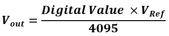
The basic formula for voltage output from the DAC is as follows:
Shown below are pin diagrams of both the most popular X Mega A1 and A4 devices. Checkout the DAC output pin locations because these are not mentioned in the reference manual.
Registers
The simplified register map for the DAC block shows that there are only a few registers to deal with. I’m not going to detail about them as the reference manuals are already doing so.
Control registers A-C are sequentially set first. These registers are responsible for selecting reference source, channel, power mode, etc. Calibration registers have names ending with “CAL” and data input registers have names ending with “DATA”. Lastly there is event system register that select which event system channel would trigger the DAC and there is a STATUS register which flags when it is possible to write new values to a specific DAC channel.
Read More: X Mega DAC